NANOIMPRINTING

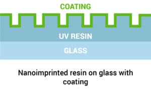
Nanoimprinting lithography (NIL) is a technology used to replicate micro- or nanometer-scale patterns from a high-resolution mold to the surface of a base substrate. The nanofabrication process involves fabricating a master mold using lithography patterning and electroforming. The patterned mold is pressed onto a substrate coated with a photosensitive resin. The nanoimprinted substrate is subsequently cured thermally or using ultraviolet light.
The nanometer-scale pattern design can be of resolution as high as 50nm (one nanometer nm is one-billionth of a meter). Nano-scale structures are replicated directly on plastic or a polymer film through thermal imprinting. For rigid substrates, the patterning technique is to nanoimprint on a resin layer bonded onto the rigid substrate. The nanoimprinted resin is UV-cured after. Examples of rigid base substrates include glass, silicon wafers or other materials.
Winovus is at the forefront of nanofabrication capabilities. We offer nano-structuring technology, including nanoimprint lithography , nanoinjection molding and customised nanopatterned mold fabrication.
Nanoimprinting functions and applications
Nanoimprint lithography (NIL) is a high-precision, cost-effective, high-throughput replication technology. The micro-and nanostructures imprinted on the flexible and rigid substrate can generate multivariate functionalities. Functionalities include superhydrophobicity, Super hydrophilicity, antireflective, high optical transmission, anti-fogging with anti-UV transmission, etc.
Nanoimprint lithography has many applications, including patterned sapphire substrates for LED, sensors, solar cells, wafer level optics (WLO), multi-lens array (MLA), and flat optics. Additional applications include diffractive optical element (DOE) for LiDar sensors, grating lens for augmented reality / virtual reality (AR/VR), and biomedical devices such as lap-on-a-chip, microarray biochips etc.

Applications of Nanoimprinting
| Display | Optics | Anti-Counterfeit | |
|---|---|---|---|
| Functions |
|
|
|
| Applications |
|
|
|
Nano-imprinting’s value-proposition
- Cost-performance advantage
- Eliminate the need for complex optical coating
- High resolution, fast processing speed and high throughput
- Compatibility with diverse materials
- Lower carbon footprint
Other nanoimprinting applications and markets include:
- Micro-arrays for genomics
- Anti-reflective optics
- Deflective optics and grating
- Diffractive optical element optics for LiDar sensors
- Surface-relief gratings
- Gratings and slant gratings for Virtual & Augmented Reality
- Medical equipment & Biotech optics
- Anti-reflection imprinted display
- Creating colors with plasmonic nanostructures
- 3D Sensors
More on Nanoimprinting
What is Nanoimprinting?
Scaling up Nanoimprinting
Nanoimprinting process on a glass substrate
UV nanoimprinting uses a photo-curable liquid resin applied to rigid or flexible substrate. The patterned mold is generally made of transparent material like a glass mold or PDMS. During imprinting, the mold and the substrate are pressed together, and the resin is UV cured to solidify it. After mold separation, the pattern is transferred onto the imprinted substrate. UV nanoimprinting uses a photo-curable liquid resin applied to rigid or flexible substrate. The patterned mold is generally made of transparent material like a glass mold or PDMS. During imprinting, the mold and the substrate are pressed together, and the resin is UV cured to solidify it. After mold separation, the pattern is transferred onto the imprinted substrate.
Thermal nanoimprinting ( also known as hot embossing) is a replication method used to imprint nanostructures directly on the surface of a polymer substrate. Amorphous and semi-crystalline thermoplastics are used for thermal nanoimprinting. They include polycarbonate (PC), polymethyl methacrylate (PMMA), polyethene (PE), polystyrene (PS), and polypropylene (PP). Nanostructures with dimensions ranging from 100nm to hundreds of microns can be imprinted.
Winovus is at the forefront of nanofabrication capabilities. We offer nano-structuring technology, including nanoimprinting , nanoinjection molding and customised nanopatterned mold fabrication.

- Master Mold fabrication
- Nickel Electroforming

- Glass substrate cleaning via oxygen plasma treatment

- Coating on glass substrate with primer resin to promote good adhesion

- Puddle dispensing of UV-Resin
- UV nanoimprinting

- Imprinted chips are coated with diamond-like-carbon (DLC) coating for scratch and chemical resistance.

- All samples are inspected for dimensional stability

Thermal nanoimprinting process on a polymer substrate

- Master Mold fabrication
- Nickel Electroforming

- Plastic substrate cleaning via oxygen plasma treatment

- Direct Thermal embossing onto the plastic substrate

- Imprinted chips are coated with diamond-like-carbon (DLC) coating for scratch and chemical resistance.

- All samples are inspected for dimensional stability

Thermal nanoimprinting ( also known as hot embossing) is a replication method used to imprint nanostructures directly on the surface of a polymer substrate. Amorphous and semi-crystalline thermoplastics are used for thermal nanoimprinting. They include polycarbonate (PC), polymethyl methacrylate (PMMA), polyethene (PE), polystyrene (PS), polypropylene (PP). Nanostructures with dimensions ranging from 100nm to hundreds of microns can be imprinted.
Examples of nanoimprinted structures

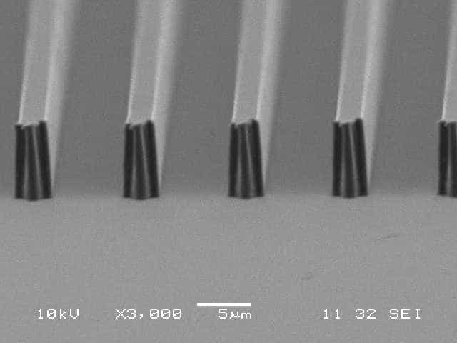
3um & 5um +ve grating

3um & 5um -ve polarity grating

3um +ve polarity grating

3um -ve polarity grating
Let us know how we can help.
Want to find out more about Winovus’ products and services?
Fill up the form below to enquire with us today.

